August 9, 2013
Desktop Printing at the Nano Level
Supported by a CBC Lever Award, Chad Mirkin’s group at NU reported July 19, 2013, in Nature Communications the development of a breakthrough lithographic tool that is capable of creating varied and complex patterns at nano-resolution on a centimeter-scale surface. This nanofabrication tool is low-cost and similar to a desktop printer. This “desktop nanofab” could enable the production of nanoscale working devices and structures at the point of use in both academia and industry.
A new low-cost, high-resolution tool is primed to revolutionize how nanotechnology is produced from the desktop, according to a new study by Northwestern University researchers.
Currently, most nanofabrication is done in multibillion-dollar centralized facilities called foundries. This is similar to printing documents in centralized printing shops. Consider, however, how the desktop printer revolutionized the transfer of information by allowing individuals to inexpensively print documents as needed. This paradigm shift is why there has been community-wide ambition in the field of nanoscience to create a desktop nanofabrication tool.
 “With this breakthrough, we can construct very high-quality materials and devices, such as processing semiconductors over large areas, and we can do it with an instrument slightly larger than a printer,” said Chad A. Mirkin, senior author of the study and a world-renowned pioneer in the field of nanoscience.
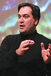
Mirkin (right) is the George B. Rathmann Professor of Chemistry in the Weinberg College of Arts and Sciences and a professor of medicine, chemical and biological engineering, biomedical engineering and materials science and engineering. He also is the director of Northwestern’s International Institute for Nanotechnology.
The study, titled “Desktop nanofabrication with massively multiplexed beam-pen lithography”, was published July 19, 2013, in Nature Communications.
The tool Mirkin’s team has created produces working devices and structures at the nanoscale level in a matter of hours, right at the point of use. It is the nanofabrication equivalent of a desktop printer.
Without requiring millions of dollars in instrumentation costs, the tool is poised to prototype a diverse range of functional structures, from gene chips to protein arrays to building patterns that control how stem cells differentiate to making electronic circuits.
“Instead of needing to have access to millions of dollars, in some cases billions of dollars of instrumentation, you can begin to build devices that normally require that type of instrumentation right at the point of use,” Mirkin said.
The paper details the advances Mirkin’s team has made in desktop nanofabrication based upon easily fabricated beam-pen lithography (BPL) pen arrays, structures that consist of an array of polymeric pyramids, each coated with an opaque layer with a 100 nanometer aperture at the tip. Using a digital micromirror device, the functional component of a projector, a single beam of light is broken up into thousands of individual beams, each channeled down the back of different pyramidal pens within the array and through the apertures at the tip of each pen.
The nanofabrication tool allows one to rapidly process substrates coated with photosensitive materials called resists and generate structures that span the macro-, micro- and nanoscales, all in one experiment.
Key advances made by Mirkin’s team include developing the hardware, writing the software to coordinate the direction of light onto the pen array and constructing a system to make all of the pieces of this instrument work together in synchrony. This approach allows each pen to write a unique pattern and for these patterns to be stitched together into functional devices.
“There is no need to create a mask or master plate every time you want to create a new structure,” Mirkin said. “You just assign the beams of light to go in different places and tell the pens what pattern you want generated.” Because the materials used to make the desktop nanofabrication tool are easily accessible, commercialization may be as little as two years away, Mirkin said. In the meantime, his team is working on building more devices and prototypes.

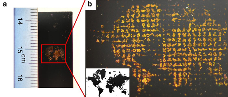
In the paper, Mirkin explains how his lab produced a map of the world (right), with nanoscale resolution that is large enough to see with the naked eye, a feat never before achieved with a scanning probe instrument. Not only that, but closer inspection with a microscope reveals that this image is actually a mosaic of individual chemical formulae made up of nanoscale points. Making this pattern showcases the instrument’s capability of simultaneously writing centimeter-scale patterns with nanoscale resolution.
Chad Mirkin is a co-recipient of a CBC Lever Award, Nanomaterials for Cancer Diagnostics and Therapeutics that matched the National Cancer Institute (NCI) award to help establish a collaborative network of Centers of Cancer Nanotechnology Excellence (CCNEs).
Adapted from: Desktop Printing at the Nano Level, by Erin White, NU News, July 19, 2013
Image Credits: Chad Mirkin (Wikimedia Commons). Figure: (a) Photographic image of an arbitrary pattern 9 × 9 mm2 in size, a portion of a ruler is shown for scale. (b) Magnified photograph of the pattern in a, with an inset depicting the image from which the mosaic was generated (adapted from Nature Communications).
This study was supported by DARPA/MTO Award N66001-08-1-2044, AOARD Award FA2386-10-1-4065, AFOSR Awards FA9550-12-1-0280 and FA9550-12-1-0141, NSF Awards DBI-1152139 and DMB-1124131, DoD/NPS/NSSEF Fellowship Awards N00244-09-1-0012 and N00244-09-1-0071, the Chicago Biomedical Consortium with support from Searle Funds at The Chicago Community Trust and a CCNE initiative of NIH Award U54 CA151880.
